{{sectionTitleLong[0]}}
Charge Densities
$ \rho_{f} $ - Free charge density (within the material), which is zero for a dielectric.
$ \rho_{sp} $ - Polarisation surface charge density, due to polarised bound charges on the surface of the material.
$ \rho_{p} $ - Polarisation charge density (within the material), which is produced due to bound charges.
Visualisation Guide
The visualisation on the right allows you to construct an arbitrary shape using small dielectric element. Press the directional buttons, the first six buttons, to add elements in specific direction. Note that you cannot overlap the elements. The surface colour shows $ \rho_{sp}: $ Red means positive surface charge, hence positive $ \rho_{sp}, $ and blue means negative surface charge, hence negative $ \rho_{sp}. $ The opacity of each of the colours shows the magnitude of $ \rho_{sp}. $ The "RESET!" button resets the number of elements to one, and "SHOW THE NORMAL VECTOR!" shows the normals vectors of each of the faces, represented by a black line. Finally, you can rotate the direction of the electric field, based in spherical polar coordinate system, by using the sliders. Note the z-axis.Current Densities
$ \textbf{J}_{sc} $ - Surface conduction current density which is due to movement of free charges, which is zero for a dielectric.
$ \textbf{J}_{m} $ - Magnetisation current density which is due to movement of bound charges within the material.
$ \textbf{J}_{sm} $ - Surface magnetisation current density which is due to movement of bound charges on the surface of the material
$ \textbf{J}_{p} $ - Polarisation current density which is due to movement of bound charges due to polarisation within the material.
The Magnetisation current density $ \textbf{J}_{m} $ is $$ \textbf{J}_{m}=\nabla \times \textbf{M}. $$ Returning to polarisation, polarisation current density can be determined by considering the time variation of $ \textbf{P}: $ $$ \textbf{J}_{p}=\frac{\partial \textbf{P}}{\partial t}=Nq\frac{\partial \textbf{d}}{\partial t}=Nq\textbf{v}. $$ This suggest that there is a variation in the dipole separation over time. Hence, the bound charges move, which produces a current density.
Visualisation Guide
The visualisation on the right allows you to construct an arbitrary shape using small dielectric element. Press the directional buttons, the first six buttons, to add elements in specific direction. Note that you cannot overlap the elements. The surface arrows shows $ \textbf{J}_{sm}. $ The arrow head is represented by a red line. The "RESET!" button resets the number of elements to one, and "SHOW THE NORMAL VECTOR!" shows the normals vectors of each of the faces, represented by a black line. Finally, you can rotate the direction of uniform magnetization, based in spherical polar coordinate system, by using the sliders. Note the z-axis. Enjoy!{{sectionTitleLong[1]}}
-
Binding Force
The actual forces between electrons and their nuclei can be complicated but we approximate it as: $$ F_{binding} = -k_{spring} x = -m \omega_0^2 x. $$ This is for small displacements, since you can expand the potential energy with a Taylor series about the equilibrium position, giving: $$ U(x) = U(0) + x U'(0) + \frac{1}{2} x^2 U''(0) + ... $$ The first term is a constant potential offset which can be ignored, and the second term can be approximated as zero around the equilibrium position. This leaves the third term which can be differentiated to give the expression for force we saw earlier, where $$ k_{spring} = U''(0). $$
-
Damping Force
As well as the restoring force there is a damping force which is partially caused by radiation emitted by the electrons. For simplicity we say that this force is opposite in direction to the velocity. It is given by $$ F_{damping} = \gamma \frac{dx}{dt} $$ where m is the mass of the electron and gamma is a proportionality constant.
-
Driving Force
The E field from an electromagnetic wave can drive the electrons, with a force of $$ F_{driving} = q E_0 cos(\omega t) $$ where $ \omega $ is the angular frequency of the light.
Electric Field in Dielectric
The dipole moment of each electron nucleus pair, is given by $ \tilde{p}(t) = q \tilde{x}(t). $ By summing these dipole moments over a volume element, we can find the polarisation of the material. $$ \tilde{\mathbf{P}} = \frac{N q^2}{m} \left(\sum_j \frac{f_i}{\omega_j^2 - \omega^2 - i \gamma_j \omega}\right) \tilde{\mathbf{E}} $$ The electric field is related to the polarisation by $$ \tilde{\mathbf{P}} = \epsilon_0 \tilde{\chi}_e \tilde{\mathbf{E}}. $$ From this we can find plane wave solutions of the E field inside the dielectric. These are: $$ \tilde{\textbf{E}}(z,t) = \tilde{\textbf{E}}_0 e^{i(\tilde{k}z-\omega t)} $$ where $ \tilde{k} $ is the complex wave number. This can be rearranged to: $$ \tilde{\textbf{E}}(z,t) = \tilde{\textbf{E}}_0(z,t) e^{-\kappa z} e^{i(kz-\omega t)} $$ where $ \kappa $ is the complex part of $ \tilde{k} $ and $ k $ is the real part.Attenuation
From the previous equation it is clear that the imaginary component of $ \tilde{k} $ will cause an exponential decay in the amplitude of the EM wave. Normally in a dielectric the imaginary component is very small, however when the frequency of the EM wave approaches the natural frequency of the electron oscillators, resonance occurs and the oscillators absorb much more energy from the wave, meaning the material becomes opaque and the imaginary component of $ \tilde{k} $ becomes significant.Most dielectrics have electron oscillators in several different environments, each having it's own natural frequency, meaning the material is opaque over a range of frequencies. Transparent materials normally have resonances in the ultraviolet part of the spectrum, rather than the visible part.
The Drude Model
The Drude Model studies the motion of electrons in material by assuming that there are only two forces on the electrons,-
electric force from applied electric field, $ \mathbf{F}_E $
-
force arises from the collisions among the electrons and between electrons and ions, $ \mathbf{F}_c $
By Newton's second law of motion, $$ m \mathbf{a} = \mathbf{F}_{total} = \mathbf{F}_E + \mathbf{F}_c $$ So, $$ m_e \frac{\partial \mathbf{v}_e}{\partial t} = -e \mathbf{E} - \frac{m_e \mathbf{v}_e}{\tau_c} $$ where $ \tau_c $ is the electron collision time.
We consider only oscillatory electric fields (or alternating current) to test the material so $ E_{applied} \propto e^{-i \omega t} $ or $ \mathbf{E} = \mathbf{E}_0 e^{-i \omega t} $, where $ \omega $ is the angular frequency of the field and $ \mathbf{E}_0 $ is real. In this case, the solution to the equation is such that $ \mathbf{v}_e \propto e^{-i \omega t} $.
Now we obtain $$ -i \omega t m_e \mathbf{v}_e = -e \mathbf{E} - \frac{m_e \mathbf{v}_e}{\tau_c} $$ so $$ \mathbf{v}_e = -\frac{e}{m_e} \frac{\tau_c}{1-i \omega \tau_c} $$ Recall that the conduction current density is given by $$ \mathbf{J}_c = N_i e \mathbf{v}_i - N_e e \mathbf{v}_e $$ where N is the number density, subscript $ i $ is for ions and $ e $ for electrons. In general, $ \mathbf{v}_e \gg \mathbf{v}_i $ given the same initial conditions for ions and electrons because ions are much heavier than electrons. We assume that the first term tends to zero so $$ \mathbf{J}_c = - N_e e \mathbf{v}_e $$ Taking the result for $\mathbf{v}_e$ from above, we get $$ \mathbf{J}_c = \frac{\sigma \mathbf{E}}{1 - i \omega \tau_c} $$ where $\sigma = \frac{N_e e^2 \tau_c}{m_e}$. We can rewrite $\mathbf{J}_c$ in terms of complex exponential form: $$ \mathbf{J}_c = \frac{\sigma}{\sqrt{1+\omega^2 \tau^2}} e^{i\tan^{-1} {(\omega \tau})} \mathbf{E} $$ The phase shift of $ \mathbf{J}_c $ to $ \mathbf{E} $ is given by $ \tan^{-1} {(\omega \tau}) $. An alternative way of looking at the phase shift between $ \mathbf{J}_c $ and $ \mathbf{E} $ is that $ \mathbf{J}_c $ is analogous to the velocity of the electrons and $ \mathbf{E} $ is analogous to the acceleration of the electrons. (In fact, it is just a matter of scaling.)
This phase shift comes out of the fact that this is effectively a damped driven harmonic oscillation. The source of the driving force is the applied electric field while the source of the damping force is the collisions between electrons or electrons and ions.
In a damped driven harmonic oscillation, the phase shift of the steady state is due to the amount of time for the transient phase to decay away.
Charge Rearrangement Time
Given some arbitrary electric field, the free electrons would rearrange themselves until the total electric field inside the conductor is 0. This arrangement happens within the charge rearrangement time $ \tau^{\star} = \frac{\epsilon}{\sigma} $, where $ \epsilon = \epsilon_0\epsilon_r $, $ \epsilon_0 $ is the permittivity of free space, $ \epsilon_r $ and $ \sigma $ are the relative permittivity and the conductivity of the material respectively. A physical insight to $ \tau^{\star} $ is that $ \epsilon $ is 'a measurement of how much the material dampens the electric field felt by the charges' while $ \sigma $ is 'a measurement as to how ready is the charge to move given some electric field'. So the charge rearrangement time $ \tau^{\star} $ is a characteristic of the conductor.The derivation, based on the Drude Model is given below: $$ \mathbf{J}_c = \frac{N_e e^2 \tau_c}{m_e \sqrt{1+\omega^2 \tau^2}} e^{i\tan^{-1} {(\omega \tau})} \mathbf{E}_{applied} $$ where $ \mathbf{E}_{applied} $ is the applied electric field. The phase shift of $ \mathbf{J}_c $ to $ \mathbf{E}_{applied} $ is given by $ \tan^{-1} {(\omega \tau}) $.
We consider only oscillatory electric fields (or alternating current) to test the material so $ \mathbf{E}_{applied} = \mathbf{E}_0 e^{-i \omega t} $, where $ \omega $ is the angular frequency of the field and $ \mathbf{E}_0 $ is real.
In a conductor, the electron collision time $ \tau_c $ is much smaller than the 'field timescale' $ T = \frac{2\pi}{\omega}, $ i.e. $ \tau_c \ll T $ or $ \frac{\tau_c}{T} \ll 1 $ so $ \omega \tau_c \ll 1. $ Taking the limits $ \omega \tau_c + 1 \rightarrow 1 $ and $ \tan^{-1} {(\omega \tau}) \rightarrow 0, $ $$ \mathbf{J}_c = \sigma \mathbf{E} $$ This is Ohm's Law.
Approximating the material to be linear, meaning that charges respond to electric fields by producing a current that is a linear function of the electric field they feel, we can use Ohm's law: $$ \mathbf{J}_c = \sigma \mathbf{E} $$ where $ \sigma $ is a constant (not a function position because we take the material to be homogeneous) scalar (not a tensor because we take the material to be isotropic).
Conservation of free charge requires $$ \frac{\partial \rho_f}{\partial t} = - \nabla \cdot \mathbf{J}_c $$ Substituting Ohm's Law for the electric field, $$ \frac{\partial \rho_f}{\partial t} = - \sigma \nabla \cdot \mathbf{E} $$ $$ = - \sigma \frac{\rho_f}{\epsilon} = - \frac{\sigma}{\epsilon} \rho_f $$ So, $$ \rho_f = \rho_{f, initial} e^{-\frac{t}{\tau^{\star}}} $$ where $ \tau^{\star} = \frac{\epsilon}{\sigma}. $
Good or Poor Conductor ?
Not to be confused with electrical conductivity, the conductivity we are talking about here is how responsive the material is to any changes in the electric field applied to it. We consider only oscillatory electric fields (or alternating current) to test the material so $ E_{applied} \propto e^{-i \omega t}, $ where $ \omega = \frac{2\pi}{T} $ is the angular frequency of the field.Now we ask the question: Are the free electrons rearranging themselves fast enough to 'cancel out' $ \mathbf{E}_{applied} $? In other words, we want to know if the timescale of electron movement is small enough relative to the timescale of the electric field changing in order for $ \mathbf{E}_{applied} $ to be cancelled out. And so an important quantity for us is the ratio of timescales $ \frac{\tau^{\star}}{T}. $ That ratio turns out to be $ \frac{\tau^{\star}}{T} = \frac{1}{2\pi} \frac{\mid \mathbf{J}_d \mid}{\mid \mathbf{J}_c \mid}, $ or $ \omega \tau^{\star} = \frac{\mid \mathbf{J}_d \mid}{\mid \mathbf{J}_c \mid} $, which is shown later.
If the free electrons take much less time than the wave period to rearrange, i.e. $ \omega \tau^{\star} \ll 1, $ then we expect the material to be a good conductor, as they can move quickly enough to cancel out the applied field. The 'good conductor' criterion depends on $ \omega $ and $ \tau^{\star} $ so it depends on both the material and the applied electric field.
The conduction current density is $$ \mathbf{J}_c = \sigma \mathbf{E}_{applied}, $$ (This is the same from the Ohm's law approximation as above)
$ \mathbf{J}_c $ is a current density due to electrons experiencing a non-zero electric field. Notice $ \sigma $ is a property of the material, which relates the electric field to the observed conduction current.
The displacement current density is $$ \mathbf{J}_d = \frac{\partial \mathbf{D}}{\partial t} = \frac{\partial }{\partial t} (\epsilon \mathbf{E}_{applied}) $$ $ \mathbf{J}_d $ is an apparent current density due to the rate of change of the electric field. Notice $ \epsilon $ is a property of the material, which relates the electric field to the observed displacement current. Notice that both the conduction current density and the displacement current density are linearly proportional to the amplitude of the applied electric field (if the field amplitude is doubled, the rate of change of the field value is also doubled). In this case, $ E_{applied} \propto e^{-i \omega t}, $ and so $$ \mathbf{J}_d = -i \omega \epsilon \mathbf{E}_{applied} $$ We only care about how quickly the field is changing and the material properties in order to classify a good or a poor conductor, not about the value of the field itself. We can achieve such a quantity by dividing the magnitudes of the two currents, as both are only linearly proportional to the electric field amplitude. $$ \frac{\mid \mathbf{J}_d \mid}{\mid \mathbf{J}_c \mid} = \frac{\omega \epsilon}{\sigma} $$ Using the charge rearrangement time $ \tau^{\star} = \frac{\epsilon}{\sigma}, $ we see $$ \frac{\omega \epsilon}{\sigma} = \omega \tau^{\star} = 2\pi \frac{\tau^{\star}}{T} $$ which is the ratio of electron movement timescale to the field timescale (period). And so $$ \frac{\omega \epsilon}{\sigma} $$ dictates whether the material is a good conductor for an EM field of that frequency.
Skin Effect
When an alternating current passes through a conductor, the alternating electric field produces an alternating magnetic field. This magnetic field in turn creates an electric field that opposes the original alternating current, known as the "back emf". The back emf is the strongest at the centre of a conductor, pushing the current to the surface of the conductor.The current diffusion equation is given by $$ \nabla^2 \mathbf{J}_c = \mu_0 \sigma \frac{\partial \mathbf{J}_c}{\partial t} $$ where $\mathbf{J}_c$ is the conduction current density in the conductor. The LHS of the above above equation gives the gradient field of the flow of current density in the conductor. The current density of an alternating current in a cylindrical wire can be written as $\mathbf{J}_c = \widetilde{J}_c (r) e^{-i \omega t} \mathbf{\hat{z}}$, which gives $$ \nabla^2 \widetilde{J}_c = -\kappa ^2 \widetilde{J}_c $$ where $ \kappa^2 = i \omega \mu_0 \sigma. $ This is a Helmholtz Equation, where $\kappa$ provides a measure of the wavenumber. Hence, $$ \kappa = \sqrt{\mu_0 \omega \sigma} \, i^{\frac{1}{2}} = \frac{1+i}{\delta} $$ where $ \delta = \sqrt{ \frac{2}{\mu_0 \sigma \omega} } $ is the skin depth, a current diffusion length scale. This means that $ J_c $ reduces by a factor of $ \frac{1}{e} $ after travelling for one $ \delta. $
Let $ a $ be the radius of a wire. If the AC frequency $ ( \omega ) $ is low, $ \delta = \sqrt{ \frac{2}{\mu_0 \sigma \omega} } \gg a $ and $ \mathbf{J}_c $ is roughly uniform throughout the wire. However, if $ \omega $ is high, $ \delta \ll a $ and $ \mathbf{J}_c $ is confined within the layer of width $ \approx \delta $ on the surface on the wire.
Based on the Drude Model, $$ \mathbf{J}_c = \frac{N_e e^2 \tau_c}{m_e \sqrt{1+\omega^2 \tau^2}} e^{i\tan^{-1} {(\omega \tau})} \mathbf{E}_{applied} $$ where $ \mathbf{E}_{applied} $ is the applied electric field. The phase shift of $ \mathbf{J}_c $ to $ \mathbf{E}_{applied} $ is given by $ \tan^{-1} {(\omega \tau}). $
We consider only oscillatory electric fields (or alternating current) to test the material so $ \mathbf{E}_{applied} = \mathbf{E}_0 e^{-i \omega t}, $ where $ \omega $ is the angular frequency of the field and $ \mathbf{E}_0. $ Taking the limits $ \omega \tau_c + 1 \rightarrow \omega \tau_c $ and $ \tan^{-1} {(\omega \tau}) \rightarrow \frac{\pi}{2}, $ $$ \mathbf{J}_c \approx \frac{N_e e^2 \tau_c}{m_e} e^{i \frac{\pi}{2}} \mathbf{E}_{applied} $$ $ E^{real} $ and $ J^{real}_c $ are out of phase by $ \frac{\pi}{2}. $
Plasmas Oscillation
Consider a cloud of neutral plasma left alone to reach its equilibrium distribution in the absence of external electromagnetic field. What happens if we displace one of the electrons in the plasma slightly? (Hint: the keywords are equilibrium and displace slightly.)The electron should be sitting at the bottom of the potential well initially. The small displacement will result in simple harmonic motion of the electron. Since plasma is a cloud of free electrons and ions, this small displacement actually causes the entire cloud to oscillate hence the collective behaviour of plasma oscillations.
It turns out that plasma oscillates at the plasma frequency: $$ \omega_p = \sqrt{\frac{N_e e^2}{m_e \epsilon_0}} $$ where $ N_e $ is the number density of electrons, $ e $ is the fundamental charge and $ \epsilon_0 $ is the permittivity of free space. Notice how the plasma frequency here depends only on the characteristics of electron distribution. This is due to the assumption that the electrons moving much faster than the positive ions in a neutral plasma.
How do we justify this assumption? Consider the lightest element, hydrogen. Ignoring the heavier isotopes, the simplest hydrogen atom consists of a proton and an electron. The mass of a proton is roughly 1800 times greater than that of an electron. Given the same initial conditions, an electron would be accelerated much more than a proton in an electric field that is not too strong. Therefore, in any plasmas, the positive ions are always much heavier than the electrons and so the movement of the positive ions can be ignored given that the electric field is not too strong.
Derivation: Displacing an electron in a neutral plasma means that the number density of electron, $ N_e $ depends on the position and time. Let $ N_e = N_0 + N_1 (x, t), $ where $ N_0 $ is the initial number density of electron and $ x $ is the direction of perturbation. Generally, the free charge density $ \rho_f $ is given by $ \rho_f = N_i e - N_e e, $ where $ N_i $ is the number density of positive ions. In this case, $ \rho_f = N_i e - (N_0 + N_1(x, t))e $ but $ N_i e = N_0 e $ for a neutral plasma so $$ \rho_f = -N_1(x, t)e $$ Also, in general, the conduction current density $ \mathbf{J}_c $ is given by $$ \mathbf{J}_c = N_i e \mathbf{v}_e - N_e e \mathbf{v}_e $$ Based on the assumption of small perturbation of electron such that the movements of positive ions can be ignored, the first term vanishes so $ \mathbf{J}_c = - N_e e \mathbf{v}_e = -(N_0 + N_1(x, t)) e \mathbf{v}_e. $ Also based on the assumption of small perturbation, $ N_0 \gg N_1, $ so $$ \mathbf{J}_c = - N_0 e \mathbf{v}_e $$ In a closed system, we require conservation of free charge, $$ \frac{\partial \rho_f}{\partial t} + \nabla \cdot \mathbf{J}_c = 0 $$ so, $$ -e\frac{\partial N_1}{\partial t} - N_0 e \nabla \cdot \mathbf{v}_e = 0 $$ Consider only in the direction of perturbation, $$ -e\frac{\partial N_1}{\partial t} - N_0 e \frac{\partial v_{e, x}}{\partial x} = 0 $$ We can rewrite this as $$ \frac{\partial v_{e, x}}{\partial x} = -\frac{1}{N_0} \frac{\partial N_1}{\partial t} $$ Assuming that $$ \frac{\partial^2 v_{e, x}}{\partial x \partial t} = \frac{\partial^2 v_{e, x}}{\partial t \partial x} $$ We get (1): $$ \frac{\partial^2 v_{e, x}}{\partial x \partial t} = -\frac{1}{N_0} \frac{\partial^2 N_1}{\partial t^2} \tag{1} $$ By Gauss' Law for electrostatics, $$ \nabla \cdot \mathbf{E} = \frac{\rho}{\epsilon_0} $$ where $ \rho = \rho_f + \rho_p, $ $ \rho_f $ is the free charge density while $ \rho_p $ is the polarisation charge density. In plasmas, $ \rho_p = 0 $ so $$ \nabla \cdot \mathbf{E} = \frac{\rho_f}{\epsilon_0} $$ From the result above, $ \rho_f = -N_1(x, t)e $ so $$ \nabla \cdot \mathbf{E} = -\frac{N_1 e}{\epsilon_0} $$ Consider only in the direction of perturbation, $$ \frac{\partial E_x}{\partial x} = -\frac{N_1 e}{\epsilon_0} $$ Now, by Newton's second law, $$ m_e \frac{\partial \mathbf{v}_e}{\partial t} = -e \mathbf{E} $$ Consider only in the direction of perturbation, $$ m_e \frac{\partial v_{e, x}}{\partial t} = -e E_x $$ So $$ \frac{\partial^2 v_{e, x}}{\partial x \partial t} = - \frac{e}{m_e} \frac{\partial E_x}{\partial x} $$ From the result for $ \frac{\partial E_x}{\partial x} $ above, we obtain (2): $$ \frac{\partial^2 v_{e, x}}{\partial x \partial t} = - \frac{e}{m_e} \cdot -\frac{N_1 e}{\epsilon_0} = \frac{e^2}{m_e \epsilon_0} N_1 \tag{2} $$ Equating (1) and (2) and rearranging the result, $$ \frac{\partial^2 N_1}{\partial t^2} + \frac{N_0 e^2}{m_e \epsilon_0} N_1 = 0 $$ This is the equation of simple harmonic motion for plasma, with a natural frequency of $$ \omega_p = \sqrt{\frac{N_0 e^2}{m_e \epsilon_0}} $$
{{sectionTitleLong[2]}}
The Key Idea
Consider an ideal dielectric (perfect insulator) that stretches to infinity. Placing it in a uniform electric field $ \mathbf{E}_{applied} $ will induce a polarisation field $ \mathbf{P} $ in it. This will give rise to a total electric field $ \mathbf{E}_{total} $ within the dielectric.In general, $ \nabla \cdot \mathbf{P} = -\rho_p, $ where $ \rho_p $ is the polarisation charge density. However, $ \nabla \times \mathbf{P} $ depends on the material.
Define the electric displacement field, $ \mathbf{D} $ as $ \mathbf{D} = \epsilon_{0}\mathbf{E}_{total} + \mathbf{P}. $ In general, $ \nabla \cdot \mathbf{D} = \rho_f, $ where $ \rho_f $ is the free charge density.
In true vacuum, where there is no dipole by definition, $$ \mathbf{P} = 0 $$ so, $$ \mathbf{D}_{vacuum} = \epsilon_{0}\mathbf{E}_{applied} $$ $$ \nabla \cdot \mathbf{D}_{vacuum} = \nabla \cdot (\epsilon_{0}\mathbf{E}_{applied}) = 0 $$ $$ \nabla \times \mathbf{D}_{vacuum} = \nabla \times (\epsilon_{0}\mathbf{E}_{applied}) = 0 $$ In a homogenous, isotropic and linear dielectric (HIL), $$ \mathbf{P} = \chi_{e}\epsilon_{0}\mathbf{E}_{total} $$ where the electric susceptibility $ \chi_{e} $ is a constant of proportionality, or $$ \mathbf{P} = \epsilon_{r}\mathbf{E}_{total} $$ where $ \epsilon_r = \chi_{e}\epsilon_{0}. $ So, \begin{align} \mathbf{D}_{dielectric} & = \epsilon_{0}(1 + \chi_{e})\mathbf{E}_{total} \\ & = \epsilon_{0}\mathbf{E}_{applied} \\ & = \mathbf{D}_{vacuum} \end{align} $$ \nabla \cdot \mathbf{D}_{dielectric} = \nabla \cdot [\epsilon_{0}(1 + \chi_{e})\mathbf{E}_{total}] = 0 $$ $$ \nabla \times \mathbf{D}_{dielectric} = \nabla \times [\epsilon_{0}(1 + \chi_{e})\mathbf{E}_{total}] = 0 $$ Note: The units of the E-field are different to those of the P and D fields, hence field line density in this visualisation only provides a qualitative representation of field strength
The Subtlety
You might notice that the total E field is weaker in a dielectric than in vacuum but the D field remains constant.A polarised material indeed weakens the total E field. However, the D field remains constant because:
-
$ \nabla \cdot \mathbf{D} = \rho_f $ and $ \rho_f $ is 0 in both the vacuum and the ideal dielectric here,
-
$ \mathbf{D} = \epsilon_{0}\mathbf{E}_{total} + \mathbf{P} $ is defined in terms of the total E field everywhere, so the reduction in total E field is complemented by the presence of P field to keep the D field constant.
Time Variant D Field
Before we talk about H field, we want to consider time variant D field. Similar to time variant E field gives rise to curl in B field, time variant D field gives rise to curl in H field. More importantly, changing this electric displacement field gives rise to displacement current density, i.e. $$ \frac{\partial \mathbf{D}}{\partial t} = \mathbf{J}_d $$The Key Idea
Consider a magnetic material that stretches to infinity. Placing it in a uniform magnetic field $ \mathbf{B}_{applied} $ will induce a magnetisation field $ \mathbf{M} $ in it. This will give rise to a total magnetic field $ \mathbf{B}_{total}. $In general, $ \nabla \times \mathbf{M} = \mathbf{J}_m, $ where $ \mathbf{J}_m $ is the magnetisation current density. However, $ \nabla \cdot \mathbf{M} $ depends on the material.
Define the magnetising field, $ \mathbf{H} $ as $ \mathbf{H} = \frac{1}{\mu_0}\mathbf{B}_{total} - \mathbf{M}, $ where $ \mu_0 $ is the permeability of free space. In general, $ \nabla \cdot \mathbf{H} = - \nabla \cdot \mathbf{M} $ and $ \nabla \times \mathbf{H} = \mathbf{J}_c + \frac{\partial \mathbf{D}}{\partial t}, $ where $ \mathbf{J}_c $ is the conduction current density. (Note: $ \frac{\partial \mathbf{D}}{\partial t} = \mathbf{J}_d $ - displacement current density.)
In a magnetic material, $ \mathbf{M} = \chi_m \mathbf{H}, $ where $ \chi_m $ is the magnetic susceptibility of the material. So, $$ \mathbf{H} = \frac{1}{\mu_0\mu_r}\mathbf{B}_{total}, $$ where $ \mu_r = 1 + \chi_m. $
Note: The units of the B-field are different to those of the M and H fields, hence field line density in this visualisation only provides a qualitative representation of field strength
The Subtlety
You might notice that the total magnetic field remaining constant when $ \mu_r $ is varied. The logic behind is similar to that of D field remains constant with varying $ \epsilon_r. $ The change in total magnetic field is complemented by the change in magnetisation field to keep the total magnetic field constant.Now let us state the Maxwell's equations (differential) in matter: $$ \nabla \cdot \mathbf{D} = \rho_f $$ $$ \nabla \cdot \mathbf{B} = 0 $$ $$ \nabla \times \mathbf{E} = -\frac{\partial \mathbf{B}}{\partial t} $$ $$ \nabla \times \mathbf{H} = \mathbf{J}_c + \frac{\partial \mathbf{D}}{\partial t} $$ We shall use these equations to study dielectrics, conductors and plasmas in the following visualisations.
{{sectionTitleLong[3]}}
When the electromagnetic wave enters the dielectric, it causes forced harmonic motion. The complex displacement of the electrons can be found by solving the forced oscillator equation (FOE): from this the dipole moment is, $$ \tilde{p}(t) = q\tilde{x}(t). $$ The electric field inside is: $$ \tilde{\textbf{E}}(z,t) = \tilde{\textbf{E}}_0(z,t) e^{-\kappa z}e^{i(kz-\omega t)} $$ with the complex wave number $$ \tilde{k} = k + i\kappa $$ The refractive index is given by: $$ \tilde{n} = \frac{c \tilde{k}}{\omega} \cong 1 + \frac{N q^2}{2m \epsilon_0} \sum_{j} \frac{f_j(\omega^2_j-\omega^2)}{(\omega^2_j-\omega^2)^2 + \gamma^2_j \omega^2} $$
$ \omega $ - Frequency of EM wave;
$ \gamma_j $ - Damping in each molecule;
$ f_j $ - No. of electrons per molecule;
$ m $ - Electron mass;
$ q $ - Electron charge;
$ N $ - No. of molecules per unit volume.
When the incoming wave has the same frequency as the natural frequency of the electrons, resonance occurs: these frequencies correspond to the points of maximum attenuation. Additionally, the real part of the refractive index changes around points of resonance. This is called anomalous dispersion.
Around these points n can become less than 1, however this is not a problem since the energy in the wave does not travel at the wave velocity, and the refractive index inside a dielectric is normally raised due to background effects.
Furthermore, since $ \tilde{k} $ can be expressed as $ \tilde{k} = Ke^{i\phi} $ and $ \tilde{\textbf{B}}_0 = \frac{Ke^{i\phi}}{ \omega} \tilde{\textbf{E}}_0. $
the B field is phase shifted, from E, by $ \phi $ inside the conductor.
The dispersion relation for a plasma is given by $$ k = \frac{\omega}{c}\Big(1 - \frac{\omega_p^2}{\omega^2}\Big)^{\frac{1}{2}}, $$ where $ c $ is the speed of light, the plasma frequency $ \omega_p = \sqrt{\frac{N_e e^2}{m_e \varepsilon_0}} $, $ N_e $ is the plasma free electron number density, e is the electron charge, $ m_e $ is the mass of an electron and $ \varepsilon_0 $ is the vacuum permittivity.
Try varying the $ N_e $ slider to in order to change $ \omega_p $. Move the $ \omega $ slider to change the frequency of the wave. Notice that when $ \omega $ is less than $ \omega_p $, the wavevector $ k $ becomes imaginary, and the wave is completely attenuated by the plasma.
The dispersion relation for a vacuum is also shown in the graph. As the number density of electrons in the plasma $ N_e $ is decreased, it becomes more like a vacuum, so it makes sense that the plasma dispersion relation should tend to the vacuum relation. Another way of thinking about it is that increasing the frequency of the wave relative to the plasma frequency (the frequency of oscillation of the electrons within the plasma) means that the electrons cannot react quickly enough to affect the wave, so the effect of passing through the plasma becomes negligible.
Derivation
To derive this dispersion relation, we start with Maxwell's equations. $$ \nabla\cdot\boldsymbol{E} = \frac{\rho_f}{\varepsilon} $$ $$ \nabla\cdot\boldsymbol{B} = 0 $$ $$ \nabla \times \boldsymbol{E} = -\frac{\partial \boldsymbol{B}}{\partial t} $$ $$ \nabla \times \boldsymbol{B} = \mu \boldsymbol{J}_c + \mu \varepsilon \frac{\partial \boldsymbol{E}}{\partial t} $$, where $ \boldsymbol{B} $ is the magnetic field, $ \boldsymbol{E} $ is the electric field, $ \mu $ is the permeability, $ \varepsilon $ is the permittivity, $ \rho_f $ is the free charge density and $ J_c $ is the conduction current density.For a plane wave, $ \nabla $ becomes $ i\boldsymbol{k} $ and $ \frac{\partial}{\partial t} $ becomes $ -i\omega. $ Therefore
Maxwell's equations become: $$ \boldsymbol{k}\cdot\boldsymbol{E} = -i\frac{\rho_f}{\varepsilon} $$ $$ \boldsymbol{k}\cdot\boldsymbol{B} = 0 $$ $$ \boldsymbol{k} \times \boldsymbol{E} = \omega \boldsymbol{B} $$ $$ \boldsymbol{k} \times \boldsymbol{B} = -i \mu_0 \boldsymbol{J}_c - \mu_0 \varepsilon \omega \boldsymbol{E} $$ In a plasma we assume that:
-
the free charge density is non zero because charge is free to move in the plasma, $\rho_f \neq 0$.
-
$\boldsymbol{J}_c = i \frac{N_e e^2}{m_e \omega}\boldsymbol{E}$
-
$\varepsilon = \varepsilon_0$
-
a plasma has no D or H fields, since a plasma is unable to be polarised.
We can now take the fourth equation, the Ampere-Maxwell equation, and substitute in our assumptions: \begin{align} \boldsymbol{k} \times \boldsymbol{B} & = -i\mu_0\Big(i\frac{N_e e^2}{m_e \omega}\boldsymbol{E}\Big) - \varepsilon_0 \mu_0 \omega \boldsymbol{E} \\ & = \varepsilon_0 \mu_0 \omega \Big(\frac{N_e e^2}{m_e \varepsilon_0 \omega^2} -1 \Big)\boldsymbol{E} \\ & = \frac{\omega}{c^2}\Big(\frac{\omega_p^2}{\omega^2} -1 \Big)\boldsymbol{E} \end{align}
where $ \omega_p = \sqrt{\frac{N_e e^2}{m_e e^2}}. $ $$ \boldsymbol{k} \times (\boldsymbol{k} \times \boldsymbol{B}) = \frac{\omega}{c^2}\Big(\frac{\omega_p^2}{\omega^2} - 1\Big)\boldsymbol{k}\times\boldsymbol{E} $$ Using an identity to rewrite the vector triple product on the left, we get $$ \boldsymbol{k}(\boldsymbol{k} \cdot \boldsymbol{B}) - \boldsymbol{B}(\boldsymbol{k} \cdot \boldsymbol{k})= \frac{\omega}{c^2}\Big(\frac{\omega_p^2}{\omega^2} - 1\Big)\boldsymbol{k}\times\boldsymbol{E}. $$ The first term on the LHS becomes zero because $ \boldsymbol{B} $ is perpendicular to $ \boldsymbol{k}, $ so this becomes $$ -k^2\boldsymbol{B} = \frac{\omega}{c^2}\Big(\frac{\omega_p^2}{\omega^2} - 1\Big)\omega\boldsymbol{B} = \Big(\frac{\omega_p^2 - \omega^2}{c^2}\boldsymbol{B}\Big) $$ $$ \Big(k^2 + \frac{\omega_p^2 - \omega^2}{c^2}\Big)\boldsymbol{B} = 0 $$ Finally, we can rearrange to get our dispersion relation for a plasma. $$ k^2 = \frac{\omega^2 - \omega_p^2}{c^2} $$ $$ k = \frac{\omega}{c}\Big(1 - \frac{\omega_p^2}{\omega^2}\Big)^\frac{1}{2} $$
{{sectionTitleLong[4]}}
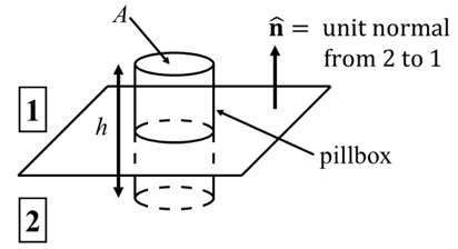
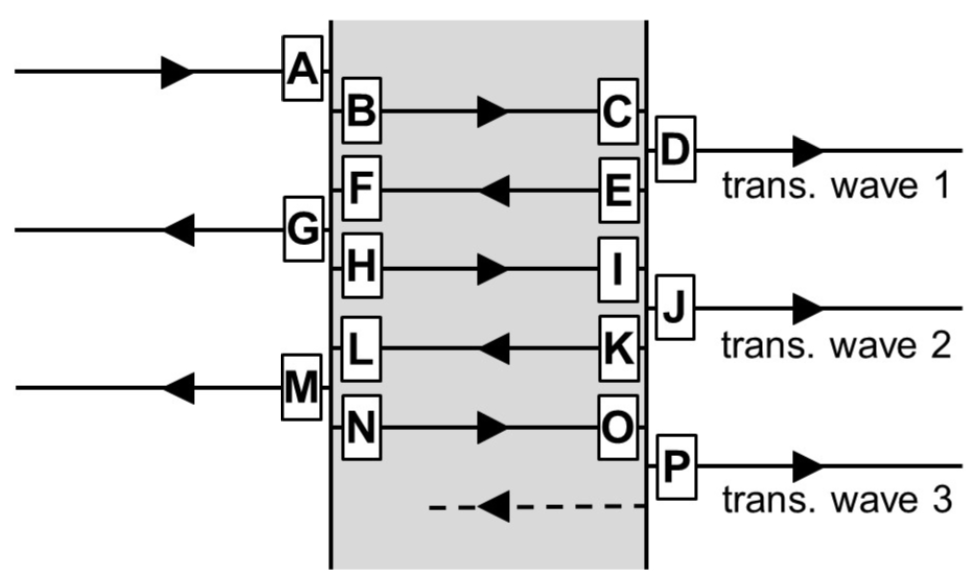
Applying the 4-field form of Maxwell’s equations on this pill-box, we arrive at 4 general boundary conditions for an EM wave incident on a dielectric boundary. The conditions can be simplified for simple media by setting $ \mu_r=1. $
P-Polarisation – here the electric field is parallel to the plane of incidence.
S-Polarised – here the opposite is true in that the electric field is perpendicular to the plane of incidence. These two linear polarisations can then form any arbitrary polarisation.
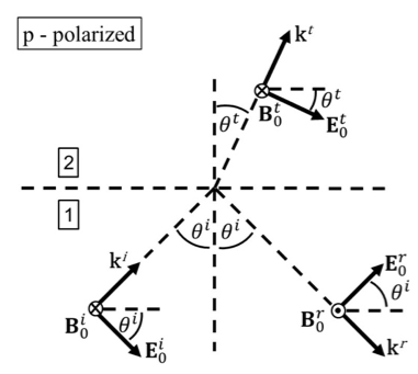
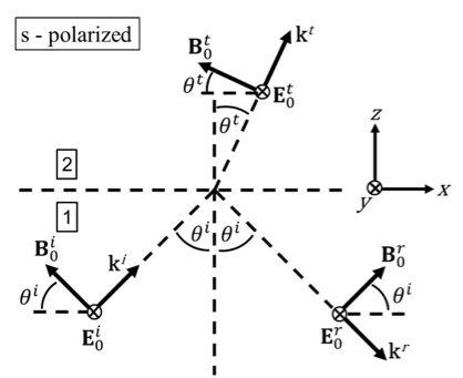
Thus, for a p-polarised incident wave, we obtain the boundary conditions $$ E_0^i\cos\theta^i+E_0^r\cos\theta^i=E_0^t\cos\theta^t $$ and $$ B_0^i-B_0^r=B_0^t. $$ We can also make use of $$ B=\frac{\mu_0E_0}{Z}, $$ where $ \mu_0 $ is the vacuum permeability and $ Z $ is the wave impedance, to write $$ B_0^i-B_0^r=B_0^t\Rightarrow\frac{E_0^i}{Z_1}-\frac{E_0^r}{Z_1}=\frac{E_0^t}{Z_2} $$ Similarly, for s-polarisation, we obtain the boundary conditions $$ E_0^i-E_0^r=E_0^t $$ and $$ -B_0^i\cos\theta^i+B_0^r\cos\theta^i=-B_0^t\cos\theta^t $$ $$ \Rightarrow\frac{E_0^i}{Z_1}-\frac{E_0^r}{Z_1}=-\frac{E_0^t}{Z_2}\cos\theta^t. $$ Finally, we make use of Snell’s law to obtain an expression for $ \theta^t $ in terms of $ \theta^i, $ to arrive at the Fresnel equations $$ t_{p,s}=\frac{E_0^t}{E_0^i}=\frac{2\cos\theta^i}{\cos\theta^{t,i}+(\frac{n_2}{n_1})\cos\theta^{i,t}} $$ and $$ r_{p,s}=\frac{E_0^r}{E_0^i}=\frac{\cos\theta^{t,i}-(\frac{n_2}{n_1})\cos\theta^{i,t}}{\cos\theta^{t,i}+(\frac{n_2}{n_1})\cos\theta^{i,t}}, $$ where $ n $ denotes the refractive index of the medium.
We now define the Brewster angle to be the angle where $ r_p=0, $ thus $ \theta_B=\arctan\frac{n_2}{n_1}. $
Also, recall that past the critical angle $ θ_c=\arcsin\frac{n_2}{n_1}, $ Snell’s law breaks down and we get total internal reflection.
But in reality, through a process that is analogous to quantum tunnelling, some of the wave does enter the second medium. This wave propagates in a direction parallel to the boundary, but decays in intensity as you move perpendicularly away from the boundary. This is an evanescent wave. (The refractive index of the material is a function of intrinsic properties of the material and the frequency of the electromagnetic wave, but we will not describe those formulae here.)
Similar to tunnelling between two potential wells in quantum mechanics, let's say there existed a material 2 of refractive index $ n_2, $ but we introduced a small gap inside of refractive index $ n_1. $ When a wave travelling in medium 2 strikes medium 1 at greater than the critical angle, total internal reflection takes place, and the transmitted wave in medium 1 decays as you move away from the boundary. But once this decaying wave hits medium 2 again, it continues propagating but with a smaller amplitude governed by how much it decayed.
The underlying maths of quantum tunnelling and the phenomenon of evanescent waves is exactly the same.
Visualisation Guide
The wave is propagating from left to right. The sliders can be varied to observe the behaviour of the incident, reflected, their combination, and the transmitted waves. Doing this, Snell's Law can be observed.To observe the phenomenon of evanescent waves, the angular frequency ratio slider should be varied until $ n2 > n1, $ and then the incident angle slider should be taken to an angle greater than the critical angle.
To understand this, consider a wave normally incident on a dielectric of thickness $ d. $ Recall that a wave can both transmit through and be reflected by a dielectric boundary. Here we label the reflection coefficient and transmission coefficient as $ r $ and $ t $ respectively.
Note that the magnitude of the reflection and transmission coefficients are the same going both from a vacuum to the dielectric and vice versa. There is, however, a $ \pi $ phase change on reflection.
It therefore follows that for any non-unity reflection coefficient, we can have an infinite number of reflections within the dielectric, with some transmission at each stage.
It can then be shown that the sum of the energies of an infinite series of transmitted waves is given by $$ E_{tot} = \frac{t'te^{i\phi}}{1-r'^2e^{2i\phi}}E^i, $$ where $ \phi=k_2d, $ $ k_2 $ is the wave vector in the dielectric and $ E^i $ is the energy of the incident wave. Note also that the prime denotes the coefficient from the dielectric to the vacuum rather than from the vacuum to the dielectric.
Thus, $$ E_{tot}=E^it'te^{i\phi}\{1+(r'e^{i\phi})^2+[(r'e^{i\phi})^2]^2+...\}. $$ Therefore, using the formula for the sum of an infinite geometric progression, we arrive at $$ E_{tot} = \frac{t'te^{i\phi}}{1-r'^2e^{2i\phi}}E^i. $$
For a more physical understanding as to why this is consider a reflection coefficient of 0.99. Under such conditions, 99% of the incident wave will be reflected at every boundary.
However, due to the $ \pi $ phase changes upon reflection, over an infinite number of reflections, the waves on the incident side of the dielectric sum to zero while the waves on the transmitted side add to the original amplitude. Thus, the net result is the entirety of the incident wave being transmitted through the dielectric.
{{sectionTitleLong[5]}}
The transmitted electromagnetic wave inside the conductor drives a conduction current in the conductor due to Ohm's Law $ (\mathbf{J}_c = \sigma \mathbf{E}^t). $ This conduction current experiences a force due to the magnetic field of the transmitted electromagnetic wave. This force acts in the same direction as the incident wave, as if the electromagnetic radiation is exerting a force on the conductor. This creates a radiation pressure by the electromagnetic radiation on the conductor, $ P_{rad}. $ In a good conductor, $ \frac{ \epsilon_0 \omega}{\sigma} \ll 1 $ and radiation pressure is given by $$ P_{rad} \approx \Big( 2 - \sqrt{ \frac{8 \epsilon_0 \omega}{\sigma} } \Big) \frac{1}{c} < S^i> $$ where $ < S^i > $ is the time average of the Poynting vector: $$ < S^i > = \frac{c \epsilon_0}{2} E^2 $$ and $ E $ is the incident electric field amplitude.
As $ \sigma \rightarrow \infty, $ $ \delta \rightarrow 0 $ and $ \sqrt{ \frac{8 \epsilon_0 \omega}{\sigma} } \rightarrow 0. $ Therefore, in a perfect conductor, $ P_{rad} = \frac{2}{c} < S^i >. $
Visualisation Guide
-
On the right, we visualise a scenario where an electromagnetic wave, travelling from left to right, is incident on a conductor. Click "Play" to begin the visualisation.
-
Switch around between the reflected and resultant waves.
-
There are 3 parameters you can change: the angular frequency of the electromagnetic wave $ \omega, $ the amplitude of the electric field $ E $ and the conductivity of the medium $ \sigma. $ Look at their effects on the skin depth, radiation pressure and the reflected wave amplitude.
-
There are certain combination of values where the reflected wave would not display. This is because the medium is no longer a good conductor $ \Big( \frac{ \epsilon_0 \omega}{\sigma} \not\ll 1 \Big). $ Hence, $ R \approx 1 - \sqrt{ \frac{8\epsilon_0 \omega}{\sigma} } $ (Hagen-Rubens Relation) is no longer applicable.
A Quantum Approach
In a wave approach, the intensity $ < S^i > $ is only dependent on the electric field amplitude of the wave. However, in a quantum perspective, $ < S^i > = N E_{photon} $ where $ N $ is the number of photons incident on the medium per unit time per unit area and $ E_{photon} = \hbar \omega $ is the energy of a single photon. Hence, $$ < S^i > = N \hbar \omega. $$ Note that $ < S^i > $ is dependent on both $ N $ and $ \omega. $ In this visualisation, we took a purely wave approach: increasing $ \omega $ does not increase the radiation pressure, as $ E $ remains unchanged. From a quantum perspective, even though the energy of each photon increases, $ N $ decreases such that intensity remains constant.Radiation pressure can be understood as the force exerted by the photons on the surface due to the change in momentum of the photons. Assuming all photons are reflected, $$ P_{rad} = 2 N \Delta p = 2 N \hbar k = 2 N \hbar \frac{\omega}{c}. $$
{{sectionTitleLong[6]}}
Plasma Critical Density
We wish to derive the equation that represents the path taken by a light ray through a plasma with an electron density and refractive index that varies with $ y. $First, we start with Snell's Law: $$ n_1\sin\alpha_1 = n_2\sin\alpha_2, $$ with the symbols defined as shown in the image.
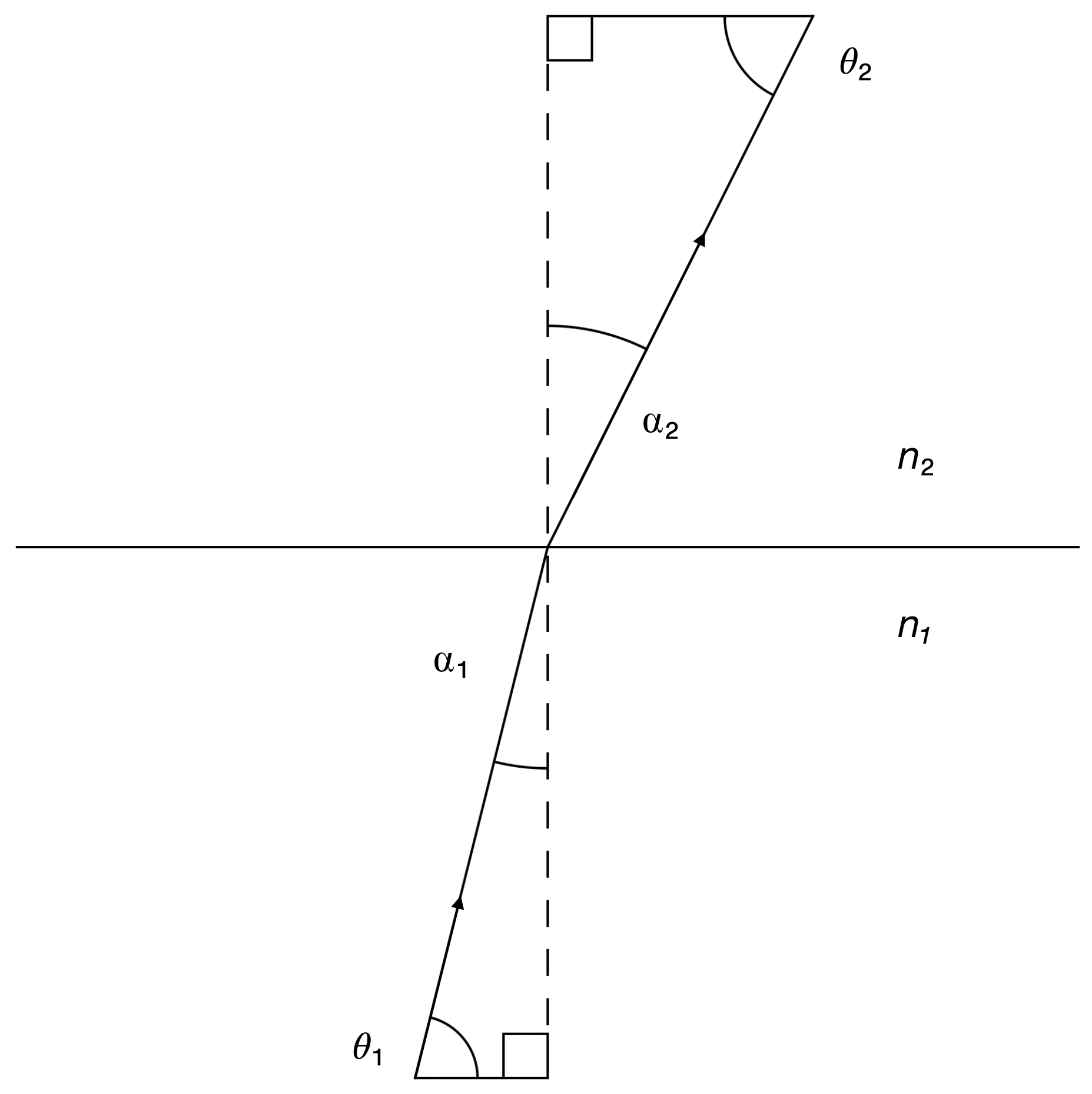
We can rewrite this in terms of $ \theta $ as $$ n_1\cos\theta_1 = n_2\cos\theta_2, $$ and then rearrange it to get $$ n_1\cos\theta_1 - n_2\cos\theta_2 = 0. $$ We can rewrite the LHS of the above equation as the change in $ n\cos\theta, $ as follows: $$ \delta(n\cos\theta) = 0. $$ Note that $ n = n(y). $
If the change in $ n\cos\theta $ is zero, then its value is constant, which we can call $ C. $ \begin{align} n(y)\cos\theta & = C \\ n(y_0)\cos\theta_0 & = C, \\ \end{align} where $ y_0 $ and $ \theta_0 $ are the initial values of $ y $ and $ \theta. $
Rearranging this equation, it is trivial to see that $$ n(y) = C\sec\theta, $$ and therefore \begin{align} \frac{dn}{d\theta}& = \frac{d}{d\theta}(C\sec\theta)\\ & = C\frac{d}{d\theta}(\sec\theta)\\ & = C\sec\theta\tan\theta\\ & = n(y)tan\theta.\\ \end{align} This can be rewritten as $$ \frac{d\theta}{dn} = \frac{1}{n\tan\theta}. $$ Using the fact that the gradient can be written as $ \frac{dy}{dx} = \tan\theta, $ we can write \begin{align} \frac{d^2y}{dx^2} & = \frac{d}{dx}(\tan\theta)\\ & = \frac{d}{dx}(\frac{1}{n}\frac{dn}{d\theta})\\ & = \frac{d}{dx}\bigg(\frac{1}{n}\bigg)\frac{dn}{d\theta} + \frac{1}{n}\frac{d}{dx}\bigg(\frac{dn}{d\theta}\bigg).\\ \end{align} Since $ n $ is a function of $ y $ only, this becomes $$ \frac{d^2y}{dx^2} = \frac{1}{n}\frac{d}{dx}\Big(\frac{dn}{d\theta}\Big), $$ which, with the help of the chain rule, becomes \begin{align} \frac{d^2y}{dx^2} & = \frac{1}{n}\frac{d}{dx}\bigg(\frac{dn}{dy}\frac{dy}{d\theta}\bigg)\\ & = \frac{1}{n}\frac{dn}{dy}\frac{d}{dx}\bigg(\frac{dy}{dx}\bigg).\\ \end{align} Since $ \frac{dy}{dx} = \tan\theta, $ it follows that $$ y = x\tan\theta + k, $$ and therefore $$ \frac{dy}{d\theta} = x\sec^2\theta. $$ We can now write \begin{align} \frac{d^2y}{dx^2} & = \frac{1}{n}\frac{dn}{dy}\frac{d}{dx}\big(x\sec^2\theta\big)\\ & = \frac{1}{n}\frac{dn}{dy}\sec^2\theta.\\ \end{align} Using Snell's Law again, we know that $ \sec\theta = \frac{n}{C}, $ so $$ \frac{d^2y}{dx^2} = \frac{1}{n}\frac{dn}{dy}\frac{n^2}{C^2} $$ $$ \frac{d^2y}{dx^2} = \frac{n}{C^2}\frac{dn}{dy} $$ But what is $ n $ for a plasma? We must use the result: $$ k = \frac{\omega}{c}\Big(1 - \frac{\omega_p^2}{\omega^2}\Big)^{\frac{1}{2}} $$ The definition of a refractive index $ n $ is $ k = \frac{\omega}{c}n, $ so $$ n = \Big(1 - \frac{\omega_p^2}{\omega^2}\Big)^{\frac{1}{2}}. $$ Given that $ \omega_p^2 = \frac{N_ee^2}{m_e\varepsilon_0}, $ we can impose a spatial gradient on the free electron density:
Let $ N_e = \gamma y $, now $$ n = \Big(1 - \frac{e^2\gamma y}{m_e\varepsilon_0\omega^2}\Big)^{\frac{1}{2}}. $$ We can take the derivative of this with respect to $ y: $ $$ \frac{dn}{dy} = -\frac{1}{2}\Big(1 - \frac{e^2\gamma y}{m_e \varepsilon_0 \omega^2}\Big)^{\frac{1}{2}}\frac{e^2}{m_e\varepsilon_0 \omega^2} $$ Multiplying $ n $ and $ \frac{dn}{dy} $ together gives $$ n\frac{dn}{dy} = -\frac{e^2 \gamma}{2m_e \varepsilon_0 \omega^2} $$ So, using an earlier result for $ \frac{d^2y}{dx^2}, $ we can now write $$ \frac{d^2y}{dx^2} = \frac{e^2\gamma}{2m_e \varepsilon_0 (C \omega)^2} $$ $$ \frac{d^2y}{dx^2} = \frac{e^2}{2m_e \varepsilon_0}\frac{\gamma}{(\omega n(y_0)\cos\theta_0)^2} $$ This is a constant! So we know that the equation for $ y $ must be $$ y(x) = \frac{e^2}{2m_e \varepsilon_0}\frac{\gamma}{(\omega n(y_0)\cos\theta_0)^2}x^2 + k_1x + k_2. $$ $ \frac{dy}{dx}\Big|_{x = 0} = \tan\theta, $ so $ k_1 = \tan\theta. $ We can also set the coordinate origin position such that $ y(0) = 0, $ meaning that $ k_2 = 0, $ so we get the final result: $$ y(x) = \frac{e^2}{2m_e \varepsilon_0}\frac{\gamma}{(\omega n(y_0)\cos\theta_0)^2}x^2 + \tan\theta_0 x $$
{{sectionTitleLong[7]}}
Click on the right to look at two applications of metamaterials in the manipulation of electromagnetic wave.
Negative Index Meta-Materials (NIMs)
NIMs are materials that have negative refractive indices for electromagnetic waves over certain frequency ranges. NIM is a composite material made from repeating unit cells stacked together. The first experimentally investigated NIM used wires and dielectrics for its unit cell.One property that NIMs can exhibit is reverse propagation. This allows for the resolution of image below the diffraction limit feasible. On top of that, the permittivity and permeability of the NIM can also be tuned by means of how the unit cells are stacked etc. Negative permittivity and permeability are also achievable in NIMs.
Meta-Material Cloaking
The manufacturing of invisibility cloaks using meta-materials that react to electromagnetic radiation in a way that conceal themselves is a focus of transformation optics. By controlling the properties of these meta-materials, light can be refracted in a way such that an "invisibility" effect can be achieved theoretically. Electromagnetic waves are typically bent around the object, and the behaviour is frequency dependent (dispersion relation). If the range of operable frequency of the material encompasses the visible spectrum, cloaking is achieved.In principle, an inhomogeneous composite meta-material can be engineered with the permittivity and permeability or any part varied at will, where they conserve the electric field vector $\mathbf{D}$, magnetic field intensity $\mathbf{B}$ and the Poynting vector $\mathbf{S}$. Such a material can concentrate electromagnetic fields in a given direction and be made to avoid or surround objects, returning to their original path without pertubation. This is consistent with the Maxwell's equations and in principle, is application to all frequencies.